
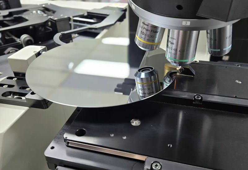
TSMC postponed the launch of High‑NA EUV, announced the A13 process, and shared plans for the end of the decade
Summary of TSMC’s plans
| Period | Process Technology | Key Features | Target Market |
|---|---|---|---|
| 2028 | A1 4‑nm (approx.) | Smartphones and consumer devices | 2029A13 – “compression” from A14, increased density by ~6% without changing design tools; Smartphones |
| 2029 | A12 – even thinner version | Transition to second‑generation GAA transistors + backside power delivery on silicon wafer; AI accelerators, high‑performance chips | |
| 2027 | A16 | First generation of GAA + backside power delivery; High‑performance computing and AI segment |
What’s new in TSMC’s plans
1. Discontinuation of High‑NA EUV until 2029
- The company announced it will not use high‑numerical‑aperture extreme ultraviolet lithography equipment for the next few years. This puts TSMC in a more confident position compared to competitors Samsung and Intel.
2. Stepwise development of process technologies
- In 2028, A14 is slated for launch, followed by two derivative variants in 2029: A13 (reduced size through optical compression) and A12 (further size reduction).
- N2, N2P, N2U, A14, and A13 are aimed at mobile chips where cost of goods sold matters.
- A16 and A12 processes target high‑performance computing and AI accelerators, prioritizing performance.
3. Second‑generation GAA transistors
- The introduction of gate‑all‑around transistor structures is planned for A14, then for A13 and A12. Backside power delivery on the silicon wafer will be used only for A12 and A16.
4. Special N2U process
- In the third year of the N2 family’s life cycle, TSMC will introduce N2U, which will increase performance by 3–4% or reduce power consumption by 8–10%, while increasing transistor density by 2–3%.
- Compatibility with existing tooling allows developers to move from N2 to N2U without significant cost. Launch is planned for 2028.
5. Timelines and updates
- A16 will be mastered in 2027 (later than originally planned).
- Serial products using the A16 technology are expected by the end of this year, but mass production will begin later.
Conclusion
TSMC demonstrates a strategy of gradual and targeted process development: from mobile chips to high‑performance computing. The company consciously abandons High‑NA EUV in the near term, focusing on more economical and flexible technologies that enable rapid adaptation to the needs of various market segments.
 Asted Cloud
Comments (0)
Share your thoughts — please be polite and stay on topic.
Log in to comment